Advanced Research & Development
MEI is actively working to expand the capability of our sensing products and to push the boundaries of emerging nanomaterials technology. Our ongoing R&D efforts are addressing both hardware and software AI to develop the next generation of sensing devices for a wide range of applications for which there are no existing solutions.
High Temperature Silicon Carbide Electronics
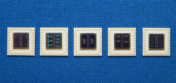
MEI is advancing the development of harsh environment SiC electronics capable of operating in high temperature and high radiation environments in excess of 500°C. MEI custom analog front signal condition application specific integrated circuits (ASICs) enable the next generation of embedded instrumentation for hypersonics, planetary research and combustion monitoring.
Wearable Sensors
MEI is developing highly sensitive and selective wearable sensors for chemical and biosensors for applications spanning from personnel protection to advanced medical/physiological monitoring. MEI sensors capable of being integrated into masks, protective clothing and person portable equipment can provide key data for assessing human exposure of chemical and environmental health threats during mission operations.
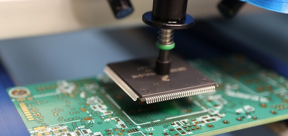
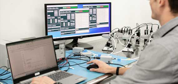
In-house and Turn Key Engineering Services
MEI has substantial in-house capability in all aspects of system design and development including: mechanical design and fabrication, PCB design/fabrication/assembly, component and material selection, chemical sensor fabrication, firmware and interface development and complete testing checkout.
Nanomaterials Research
Our nanomaterials research work is opening new vistas of applications ranging from advanced catalysts and reactive micro fluidic systems to biological and chemical sensing. The use of engineered nanostructures provides enhanced chemical sensitivity and selectivity.
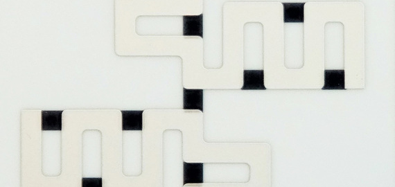
Passive Wireless Sensors
MEI has developed 2-D and 3-D passive antenna fabrication technology using non-standard, additive manufacturing processes. These RF structures can be coupled with embedded chemical sensors (measuring, for example, gas concentration, pH and conductivity) or physical sensors (measuring, for example, pressure, temperature and strain) to form comprehensive passive wireless sensor networks. These highly miniaturized wireless sensors can be used for many applications including non-destructive testing, in-situ health monitoring and remote environmental monitoring. Large networks of RF coupled sensors can be deployed and combined with MEI’s machine learning applications for real-time monitoring of structures, aerospace vehicles, remediation sites and energy production wells.
Data Fusion and Machine Learning Software Development
Leveraging our experience with large complex data sets, MEI has developed advanced data fusion algorithms to identify key signal attributes and associations for real-time AI decision making by autonomous agents.
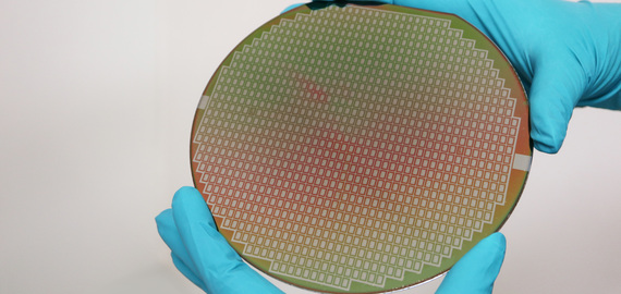
Micro/Nano Fabrication Research
MEI is engaged in micro and nano fabrication research ranging from including patterning, atomic layer deposition processing, DC and RF sputtering of exotic and non-standard materials, and full back-end packaging of custom sensor devices.
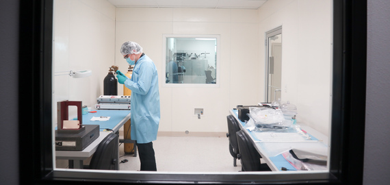
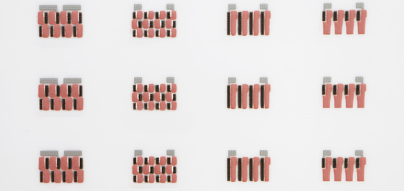
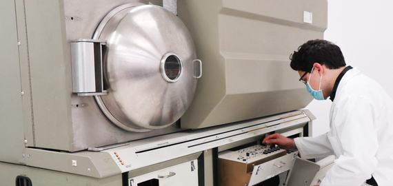
Precision Assembly and Testing Services
MEI has a full array of in-house, MIL-Standard testing capability including vibration, thermal cycle, EMI/EMC, proof and leak and altitude testing. MEI precision assembly cleanrooms meet spaceflight standards to support full development of customer hardware.